Gul 1
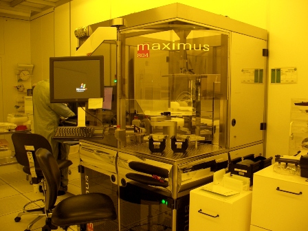
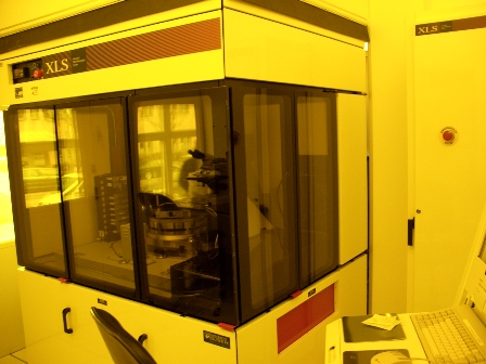
In the photolithography area light is used to transfer a geometric pattern from a photo mask to a light-sensitive chemical photoresist on the substrate.
 |
The wafer is covered with photo resist by spin coating (left) and
then exposed in a stepper using ultraviolet light.(right)
|
 |
All pictures can be viewed in larger format, just click on them.
Return to start of Virtual Clean Room Lab Tour